New Business Field

Life Science-Related MaterialsPhoto Patternable Permanent Materials for Structure Fabrication/ Photo Patternable Adhesives Materials
Negative tone photo patterable permanent film with high resolution and high adhesion, enabling the formation of high aspect ratio patterns for MEMS (Dry film and liqud type)
Pattern & Adhesive in One Material
Features
- These photoresists provide a negative photosensitive permanent film with high resolution and high adhesion, enabling the formation of high aspect ratio patterns.
- We have two types: liquid type(TMMR® S2000) and film type(TMMF® S2000).If combined, it is possible to form of hollow structures through the tenting process using film photoresists.
- Compared with conventional the sacrificial layer process, these photoresists enable significant process simplification.
- Low cytotoxicity*
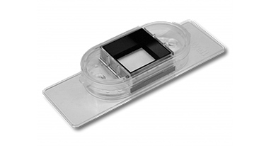
- Photo Patternable Adhesive Materials for Wafer-Level Microfluidic Device Fabrication
- Enable to make patterns by photolithography process
- Permanent resist with high adhesive property
- Low autofluorescence, Low cytotoxicity*
* Cytotoxicity was tested according to the ISO 10993-5 standard. IC50 (50% inhibitory concentration) : >100%

Hollow structure forming
- TMMF® S2000 Series:Film type photoresist
- TMMR® S2000 Series:Liquid type photoresist

Applications
- MEMS (Micro Electro Mechanical Systems)
- Biochips (Microfluidics: μTAS, Lab on a chip)
Post Cured Film Performance / Chemical Resistance
Post Cured Film Performance
| Physical properties | Measurement | TMMF®S2000 & TMMR®S2000 | |
|---|---|---|---|
| Tg (℃) | DMA | 230 | |
| CTE (ppm/℃) | TMA | 65 | |
| Tensile strength (MPa) | Tension | 60.3 | |
| Elongation (%) | 4.4 | ||
| Young’s modulus (GPa) | 2.1 | ||
| 5% Thermal decomposition (℃) | TG/DTA | 320 | |
| Vickers Hardness (HV) | Push-In | 28.1 | |
| Martens Hardness (N/㎟) | 199 | ||
| Young’s modulus (GPa) | 3.8 | ||
| Water absorption (%) | 23 ℃-24 h dipping | 1.8 | |
| Transmittance (%) | 500 nm | UV | 93 |
| 600 nm | 95 | ||
| 700 nm | 98 | ||
| 800 nm | 99 | ||
Post Cure Chemical Resistance
| Category | Chemical | Dipping | Result |
|---|---|---|---|
| Solvent | NMP | 80 ℃-15 min | No change |
| GBL | 80 ℃-15 min | No change | |
| EL | 23 ℃-15 min | No change | |
| Acetone | 23 ℃-15 min | No change | |
| PGMEA | 23 ℃-15 min | No change | |
| IPA | 23 ℃-15 min | No change | |
| DMSO | 80 ℃-15 min | No change | |
| Alkaline solution | 25% NaOH | 40 ℃-10 min | No change |
| 10% KOH | 40 ℃-10 min | No change | |
| TMAH 2.38% | 40 ℃-10 min | No change | |
| Acid solution | H2SO4/H2O2 | 40 ℃-10 min | No change |
| 1% HF | 23 ℃-5 min | No change |
Post Cured Film Performance
| Physical properties | Measurement | Photo Patternable Adhesive | |
|---|---|---|---|
| Tg (℃) | DMA | 97 | |
| CTE (ppm/℃) | TMA | 63 | |
| Tensile strength (MPa) | Tensile | 39.8 | |
| Elongation (%) | 5.5 | ||
| Young’s modulus (GPa) | 1.67 | ||
| 5% Thermal decomposition (℃) | TG/DTA | 399 | |
| Transmittance (%) | 400 nm | UV | 84.7 |
| 500 nm | 99.1 | ||
| 600 nm | 99.2 | ||
| 700 nm | 99.2 | ||
Post Cure Chemical Resistance
| Category | Chemical | Dipping | Result |
|---|---|---|---|
| Solvent | NMP | 23 ℃-15 min | No change |
| GBL | 23 ℃-15 min | No change | |
| EL | 23 ℃-15 min | No change | |
| Acetone | 23 ℃-15 min | No change | |
| PGMEA | 23 ℃-15 min | No change | |
| IPA | 23 ℃-15 min | No change | |
| DMSO | 80 ℃-15 min | No change | |
| Alkaline solution | 5% KOH | 40 ℃-10 min | No change |
| TMAH 2.38% | 40 ℃-10 min | No change | |
| Acid solution | 1% HF | 23 ℃-5 min | No change |
References
High-resolution permanent photoresist laminate for microsystem applications, J. Micro/Nanolith. MEMS MOEMS 7 (3), 2008, 033009-1-6
Dry Film Resist Microfluidic Channels on Printed Circuit Board and its Application as Fluidic Interconnection for Nanofluidic Chips: Fabrication Challenges, ICQNM 2011 : The Fifth International Conference on Quantum, Nano and Micro Technologies, 71-76
High-resolution permanent photoresist laminate TMMF for sealed microfluidic structures in biological applications, J. Micromech. Microeng, 21(2011), 1-9
HYBRID FABRICATION OF MICROFLUIDIC CHIPS BASED ON COC, SILICON AND TMMF DRY RESIST, Tech Dig IEEE Micro Electro Mech Syst, 23rd Vol.1, 2010, 400-403
Lab-on-a-Foil: microfluidics on thin and flexible films, Lab Chip, 2010, 10, 1365-1386
Low-Cost Technology for the Integration of Micro- and Nanochips into Fluidic Systems on Printed Circuit Board: Fabrication Challenges, International Journal on Advances in Systems and Measurements, vol 5 no 1 & 2, 2012, 11-21
Picoliter Droplet Dispenser with Integrated Impedance Detector for Single-cell Printing, ACTUATOR 2012, 13th International Conference on New Actuators, 18-20 June 2012, 418-421
Product Inquiry
If you have any inquiries about this product, please click the button below. Our representative will contact you by return.